US 12,074,303 B2
Electrode for use in a layered device structure, as well as a battery device
Jan Eite Bullema, Helmond (NL); Cornelius Maria Rops, Waarle (NL); and Maurice Pierre Marie Arthur Limpens, Elsloo (NL)
Assigned to Nederlandse Organisatie voor toegepast-natuurwetenschappelijk onderzoek TNO, 's-Gravenhage (NL)
Appl. No. 17/259,321
Filed by Nederlandse Organisatie voor toegepast-natuurwetenschappelijk onderzoek TNO, 's-Gravenhage (NL)
PCT Filed Jul. 12, 2019, PCT No. PCT/NL2019/050437
§ 371(c)(1), (2) Date Jan. 11, 2021,
PCT Pub. No. WO2020/013695, PCT Pub. Date Jan. 16, 2020.
Claims priority of application No. 18183227 (EP), filed on Jul. 12, 2018.
Prior Publication US 2021/0159560 A1, May 27, 2021
Int. Cl. H01M 10/6556 (2014.01); H01M 10/613 (2014.01); H01M 10/647 (2014.01); H01M 10/654 (2014.01); H01M 10/6569 (2014.01); H01M 4/02 (2006.01); H01M 50/103 (2021.01); H01M 50/107 (2021.01)
CPC H01M 10/6556 (2015.04) [H01M 10/613 (2015.04); H01M 10/647 (2015.04); H01M 10/654 (2015.04); H01M 10/6569 (2015.04); H01M 2004/021 (2013.01); H01M 50/103 (2021.01); H01M 50/107 (2021.01)] 19 Claims
OG exemplary drawing
 
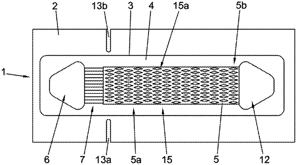
1. An electrode for use in a layered device structure, the electrode comprising:
at least one layer of conductive material; and
at least one micro evaporator having an evaporator inlet for receiving a cooling fluid and an evaporator outlet for removing the cooling fluid after evaporation,
wherein each one of the at least one micro evaporator includes a plurality of micro channels forming an evaporation volume, and
wherein each of the plurality of micro channels is embedded in the at least one layer of conductive material.