| CPC H01L 33/54 (2013.01) [H01L 25/167 (2013.01); H01L 33/62 (2013.01); H01L 33/20 (2013.01); H01L 33/56 (2013.01); H01L 2933/0066 (2013.01)] | 20 Claims |

|
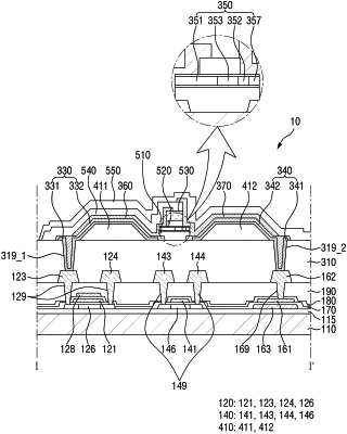
1. A display device comprising:
a first electrode;
a second electrode facing the first electrode;
a first insulating layer on the first electrode and the second electrode and positioned between the first electrode and the second electrode;
a light emitting element on the first insulating layer;
a second insulating layer covering the light emitting element and exposing first and second end portions of the light emitting element;
a third insulating layer on the second insulating layer;
a first contact electrode electrically connected to the first electrode, the first contact electrode being on the third insulating layer and in contact with the first end portion of the light emitting element exposed by the second insulating layer; and
a second contact electrode electrically connected to the second electrode, the second contact electrode being on the third insulating layer and in contact with a second end portion of the light emitting element exposed by the second insulating layer.
|