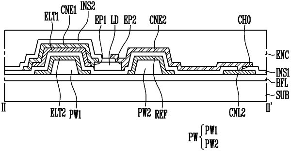
| CPC H01L 33/38 (2013.01) [H01L 25/0753 (2013.01); H01L 25/167 (2013.01); H01L 33/62 (2013.01); H01L 2933/0066 (2013.01)] | 19 Claims |

|
1. A light emitting device comprising:
at least one first electrode and at least one second electrode disposed on different layers on a substrate;
a first insulating layer disposed between the at least one first electrode and the at least one second electrode; and
at least one light emitting diode electrically connected between the at least one first electrode and the at least one second electrode, the at least one light emitting diode being rod shaped and having a length extending in a longitudinal direction parallel with a main surface of the substrate, the length being a longest dimension of the at least one light emitting diode wherein
the at least one first electrode is disposed on the first insulating layer, and
the at least one second electrode is disposed between the substrate and the first insulating layer to overlap the at least one first electrode.
|