US 12,074,254 B2
Nitride semiconductor device and substrate thereof, method for forming rare earth element-added nitride layer, and red-light emitting device and method for manufacturing the same
Shuhei Ichikawa, Suita (JP); Yasufumi Fujiwara, Suita (JP); and Jun Tatebayashi, Suita (JP)
Assigned to OSAKA UNIVERSITY, Suita (JP)
Appl. No. 17/271,173
Filed by OSAKA UNIVERSITY, Suita (JP)
PCT Filed Aug. 30, 2019, PCT No. PCT/JP2019/034070
§ 371(c)(1), (2) Date Feb. 24, 2021,
PCT Pub. No. WO2020/050159, PCT Pub. Date Mar. 12, 2020.
Claims priority of application No. 2018-164868 (JP), filed on Sep. 3, 2018; and application No. 2019-029938 (JP), filed on Feb. 22, 2019.
Prior Publication US 2021/0399175 A1, Dec. 23, 2021
Int. Cl. H01L 33/32 (2010.01); H01L 33/00 (2010.01); H01L 33/02 (2010.01); H01L 33/16 (2010.01)
CPC H01L 33/325 (2013.01) [H01L 33/007 (2013.01); H01L 33/0075 (2013.01); H01L 33/025 (2013.01); H01L 33/16 (2013.01)] 22 Claims
OG exemplary drawing
 
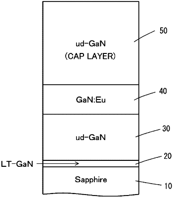
1. A nitride semiconductor device configured by providing a nitride semiconductor layer on a substrate, characterized in that
the substrate is an off-angle inclined substrate,
a rare earth element-added nitride layer to which a rare earth element is added is provided on the substrate as a base treatment layer to prevent the occurrence of a macro step and to flatten a surface, and
a nitride semiconductor layer is provided on the rare earth element-added nitride layer.