| CPC H01L 33/12 (2013.01) [H01L 33/007 (2013.01); H01L 33/06 (2013.01); H01L 33/08 (2013.01); H01L 33/24 (2013.01); H01L 33/32 (2013.01); H01L 33/405 (2013.01); H01L 33/44 (2013.01); H01L 2933/0016 (2013.01); H01L 2933/0025 (2013.01)] | 19 Claims |

|
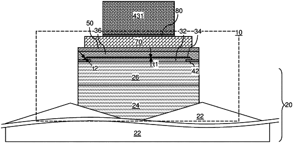
1. A light emitting diode (LED) structure, comprising:
a semiconductor buffer layer comprising a III-nitride semiconductor material;
an n-doped semiconductor material layer;
a stress relaxation layer having a thickness of 0.5 nm or less having a first surface contacting the semiconductor buffer layer and a second surface contacting the n-doped semiconductor material layer;
an anode contact; and
a reflector,
wherein:
the n-doped semiconductor material layer is located between the anode contact and the stress relaxation layer;
the anode contact is located between the reflector and the n-doped semiconductor material layer, and
the LED structure comprises a sidewall extending continuously in a direction perpendicular to the first surface and the second surface of the stress relaxation layer along an entire thickness of the n-doped semiconductor material layer, an entire thickness of the stress relaxation layer, and at least a portion of a thickness of the semiconductor buffer layer.
|