| CPC H01L 33/06 (2013.01) [H01L 33/005 (2013.01); H01L 33/14 (2013.01); H10K 50/15 (2023.02); H10K 71/00 (2023.02)] | 16 Claims |

|
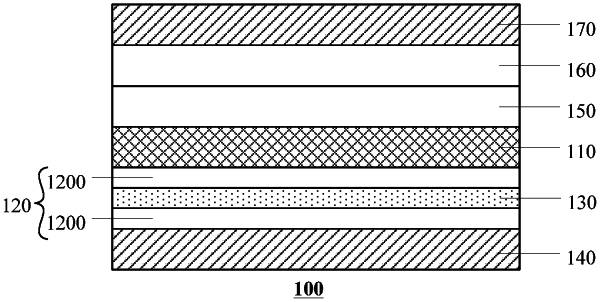
1. A quantum dot light emitting structure, comprising:
a quantum dot light emitting layer;
an electrode; and
an electron transport layer located between the quantum dot light emitting layer and the electrode,
wherein the quantum dot light emitting structure further comprises an electron blocking layer located in the electron transport layer,
the electron transport layer comprises a first electron transport sub-layer and a second electron transport sub-layer, the second transport sub-layer is arranged on a side, close to the quantum dot light emitting layer, of the first electron transport sub-layer, and an energy level of conduction band minimum of the second electron transport sub-layer is greater than that of the first electron transport sub-layer and less than an energy level of conduction band minimum of the quantum dot light emitting layer, the second electron transport sub-layer comprises a plurality of doped electron transport sub-layers,
the electron blocking layer comprises a first electron blocking sub-layer and a second electron blocking sub-layer, the first electron blocking sub-layer is located between the first electron transport sub-layer and the second electron transport sub-layer, and the second electron blocking sub-layer is located between two of the plurality of doped electron transport sub-layers in the second electron transport sub-layer.
|