| CPC H01L 31/1075 (2013.01) [H01L 31/02162 (2013.01); H01L 31/03046 (2013.01); H01L 31/1844 (2013.01); H01L 31/1852 (2013.01); H01L 31/1876 (2013.01)] | 13 Claims |
|
1. A method for packaging an avalanche photodiode, comprising:
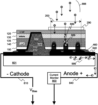
on a semiconductor wafer comprising epitaxial layers for fabricating one or more avalanche photodiodes, wherein the epitaxial layers include an n-doped InP layer and the semiconductor wafer additionally has regions of p-doped InP material,
etching at least one well into the semiconductor wafer,
wherein the well extends from a first surface of the wafer to the n-doped InP layer;
forming, on the first surface of the semiconductor wafer,
a first electrical contact structure that electrically connects through the at least one well to the n-doped InP layer;
forming, on the first surface of the semiconductor wafer,
a second electrical contact structure, electrically separated from the first contact structure, that electrically connects to the p-doped InP material;
bonding the semiconductor wafer to a support structure,
the support structure comprising:
at least one electrical contact positioned to align with the first electrical contact structure on the first surface of the semiconductor wafer, and
at least one electrical contact positioned to align with the second electrical contact structure on the first surface of the semiconductor wafer;
thinning the semiconductor wafer on a second surface of the wafer opposite the first surface of the wafer to expose the n-doped InP layer;
depositing an anti-reflection coating onto a portion of the exposed n-doped InP layer corresponding to an avalanche photodiode structure; and
dicing the bonded wafer and support structure.
|