| CPC H01L 31/107 (2013.01) [H01L 27/14612 (2013.01); H01L 27/14643 (2013.01); H04N 25/705 (2023.01); H04N 25/75 (2023.01)] | 15 Claims |

|
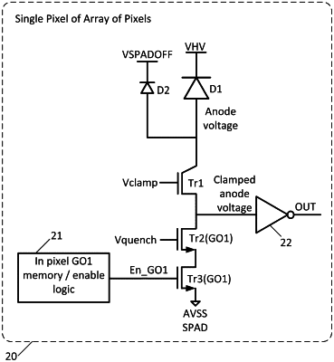
1. An array of pixels, each pixel comprising:
a single photon avalanche diode (SPAD);
a transistor circuit comprising:
a clamp transistor configured to clamp an anode voltage of the SPAD to be no more than a threshold clamped anode voltage; and
a quenching element coupled in series with the clamp transistor and configured to quench the anode voltage of the SPAD when the SPAD is struck by an incoming photon; and
readout circuitry coupled to receive the clamped anode voltage from the transistor circuit and configured to generate a pixel output therefrom, wherein the threshold clamped anode voltage is below a maximum voltage rating of transistors forming the readout circuitry.
|