| CPC H01L 31/0512 (2013.01) [H01L 31/0201 (2013.01); H01L 31/0488 (2013.01); H01L 31/0508 (2013.01); H01L 31/0547 (2014.12)] | 9 Claims |

|
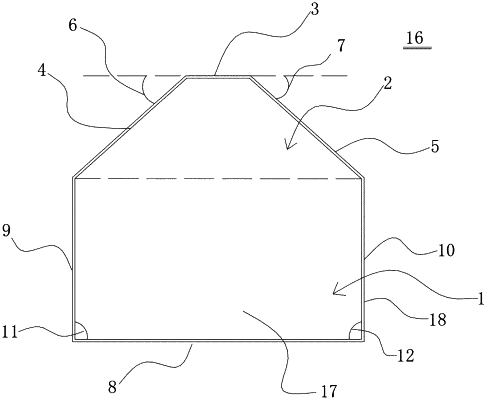
1. A solder strip, wherein the solder strip comprises a main body section and a flat section connected to the main body section, a cross-section of the main body section of the solder strip comprises a base portion and a reflective portion arranged above the base portion;
the reflective portion includes a top edge, a first side edge and a second side edge, one end of the first side edge and one end of the second side edge continue from the top edge, and the other end of the first side edge and the other end of the second side edge continue from the base portion; and
a first angle is formed between the first side edge and an extension line of a bottom edge of the base portion, a second angle is formed between the second side edge and the extension line of the bottom edge of the base portion, and the first angle and the second angle are both acute angles formed in a range greater than 42.5°,
wherein a height of the cross-section of the solder strip is less than or equal to 0.3 mm,
wherein the base portion has a width of 0.4±0.1 mm and a height of 0.18±0.02 mm, and the reflective portion has a height of 0.09±0.01 mm,
wherein the solder strip comprises a copper substrate and a solder layer coated on a surface of the copper substrate, and
wherein the solder layer has a thickness in a range of 10 μm to 15 μm,
wherein the first side edge or the second side edge includes at least three continuous folded sections, and an angle formed between each section of the at least three continuous folded sections and the extension line of the bottom edge of the base portion is an acute angle greater than 42.5°.
|