| CPC H01L 31/02167 (2013.01) [H01L 31/02168 (2013.01); H01L 31/022441 (2013.01); H01L 31/02363 (2013.01); H01L 31/028 (2013.01); H01L 31/0288 (2013.01); H01L 31/03682 (2013.01); H01L 31/03762 (2013.01); H01L 31/0682 (2013.01); H01L 31/182 (2013.01); H01L 31/1868 (2013.01); H01L 31/202 (2013.01); Y02E 10/546 (2013.01); Y02E 10/547 (2013.01); Y02E 10/548 (2013.01); Y02P 70/50 (2015.11)] | 18 Claims |

|
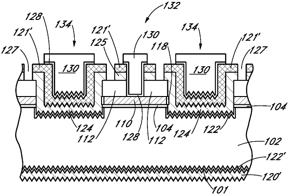
1. A solar cell, comprising:
a semiconductor substrate having a light-receiving surface and a back surface, the back surface below the light-receiving surface;
an N-type emitter region disposed on the back surface of the semiconductor substrate, wherein the N-type emitter region is a planar layer;
a P-type emitter region disposed on the back surface of the semiconductor substrate, the P-type emitter region comprising polycrystalline silicon having hydrogen therein, and the P-type emitter region electrically insulated and physically isolated from the N-type emitter region by a single dielectric material, the single dielectric material in direct physical contact with the P-type emitter region and with the N-type emitter region, and the single dielectric material confined to sidewalls of the N-type emitter region, wherein the P-type emitter region is a non-planar layer, and wherein the P-type emitter region has an uppermost surface above an uppermost surface of the N-type emitter region, and the P-type emitter region has a bottommost surface below a bottommost surface of the N-type emitter region;
a passivation layer disposed on the P-type emitter region but not on the N-type emitter region, the passivation layer comprising amorphous silicon having hydrogen therein, the passivation layer covering an entirety of a side of the P-type emitter region opposite the semiconductor substrate;
a first conductive contact structure electrically connected to and in direct contact with the N-type emitter region; and
a second conductive contact structure electrically connected to the P-type emitter region and in direct contact with the passivation layer, wherein the second conductive contact structure has an uppermost surface below the uppermost surface of the N-type emitter region, wherein the second conductive contact is physically separated from an entirety of the P-type emitter region by the passivation layer.
|