US 12,074,225 B2
PIN diodes with multi-thickness intrinsic regions
Timothy Edward Boles, Tyngsboro, MA (US); James Joseph Brogle, Merrimac, MA (US); Joseph Gerard Bukowski, Derry, NH (US); and Margaret Mary Barter, Lowell, MA (US)
Assigned to MACOM TECHNOLOGY SOLUTIONS HOLDINGS, INC., Lowell, MA (US)
Appl. No. 17/289,990
Filed by MACOM Technology Solutions Holdings, Inc., Lowell, MA (US)
PCT Filed Dec. 2, 2019, PCT No. PCT/US2019/064018
§ 371(c)(1), (2) Date Apr. 29, 2021,
PCT Pub. No. WO2020/117679, PCT Pub. Date Jun. 11, 2020.
Claims priority of provisional application 62/774,577, filed on Dec. 3, 2018.
Prior Publication US 2021/0399143 A1, Dec. 23, 2021
Int. Cl. H01L 29/868 (2006.01); H01L 21/265 (2006.01); H01L 29/06 (2006.01); H01L 29/66 (2006.01)
CPC H01L 29/868 (2013.01) [H01L 21/26513 (2013.01); H01L 29/0688 (2013.01); H01L 29/6609 (2013.01)] 20 Claims
OG exemplary drawing
 
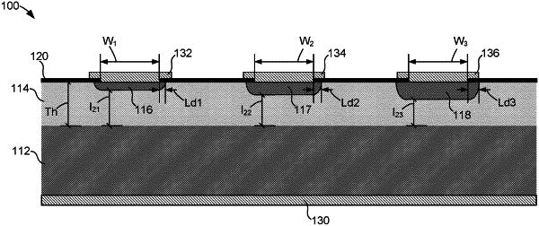
1. A semiconductor structure of diodes, comprising:
an N-type silicon substrate;
an intrinsic layer on the N-type silicon substrate, the intrinsic layer comprising an undoped silicon layer;
a first P-type region for a first PIN diode, the first P-type region extending from a top surface of the intrinsic layer into the intrinsic layer and to a first depth in the intrinsic layer; and
a second P-type region for a second PIN diode, the second P-type region extending from a top surface of the intrinsic layer into the intrinsic layer and to a second depth in the intrinsic layer, wherein the first depth is greater than the second depth.