| CPC H01L 29/78633 (2013.01) [H01L 27/1225 (2013.01); H01L 27/124 (2013.01); H01L 27/127 (2013.01); H01L 27/1288 (2013.01); H01L 29/66969 (2013.01); H01L 29/7869 (2013.01)] | 16 Claims |

|
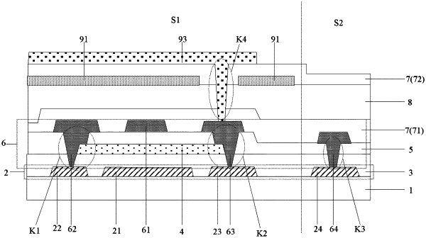
1. An array substrate, comprising a display area and a non-display area located at a periphery of the display area, wherein the array substrate comprises:
a base substrate;
a first metal layer located at one side of the base substrate, the first metal layer comprises a light shielding part, a source and a drain, the light shielding part, the source and the drain are located in the display area;
a buffer layer located at a side, facing away from the base substrate, of the first metal layer;
an active layer located at a side, facing away from the first metal layer, of the buffer layer and located in the display area;
a gate insulating layer located at a side, facing away from the buffer layer, of the active layer; and
a second metal layer located at a side, facing away from the active layer, of the gate insulating layer, wherein the second metal layer comprises a gate, a source landing electrode and a drain landing electrode, the source landing electrode is in contact with the active layer and the source through a first via hole exposing one end of the active layer, and the drain landing electrode is in contact with the active layer and the drain through a second via hole exposing the other end of the active layer;
wherein a quantity of layers through which the first via hole penetrates is equal to a quantity of layers through which the second via hole penetrates;
wherein the first metal layer further comprises a first signal line located in the non-display area; and
the second metal layer further comprises a second signal line located in the non-display area, wherein the second signal line and the first signal line are conductive through a third via hole penetrating through the gate insulating layer and the buffer layer.
|