| CPC H01L 29/78633 (2013.01) [H01L 25/075 (2013.01); H01L 27/1225 (2013.01); H01L 27/127 (2013.01); H01L 29/66969 (2013.01); H01L 29/7869 (2013.01)] | 12 Claims |

|
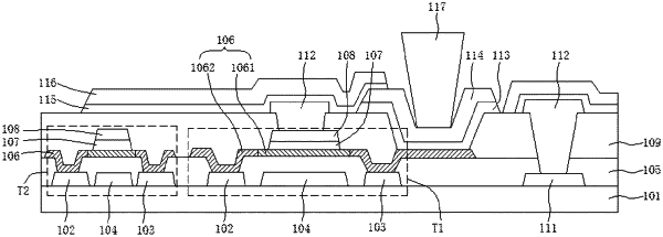
1. An array substrate, wherein the array substrate comprises:
an underlay;
a source electrode disposed on the underlay;
a drain electrode disposed on the underlay;
a light shielding portion disposed on the underlay; and
an active layer disposed correspondingly on the source electrode, the drain electrode, and the light shielding portion, wherein the active layer comprises a channel region;
wherein the light shielding portion corresponds to the channel region, the source electrode, the drain electrode, and the light shielding portion are disposed in a same layer, and a material of the source electrode and the drain electrode is same as a material of the light shielding portion;
wherein the active layer further comprises a non-channel region located on two sides of the channel region, and the source electrode and the drain electrode contact the non-channel region;
wherein the array substrate further comprises a top gate, the top gate is located on the active layer, and the top gate is disposed to correspond to the channel region of the active layer;
wherein the light shielding portion is disposed at an interval from the source electrode and is disposed at an interval from the drain electrode, and the light shielding portion is disposed opposite rightly to the top gate; or, the light shielding portion is connected to at least one of the source electrode and the drain electrode;
wherein the top gate is electrically connected to the light shielding portion through a via hole.
|