| CPC H01L 29/78618 (2013.01) [H01L 21/823807 (2013.01); H01L 21/823814 (2013.01); H01L 21/823828 (2013.01); H01L 21/823885 (2013.01); H01L 27/092 (2013.01); H01L 29/41741 (2013.01); H01L 29/42392 (2013.01); H01L 29/66356 (2013.01); H01L 29/66666 (2013.01); H01L 29/7391 (2013.01); H01L 29/7788 (2013.01); H01L 29/78642 (2013.01); H01L 29/78696 (2013.01); H01L 21/823487 (2013.01)] | 20 Claims |

|
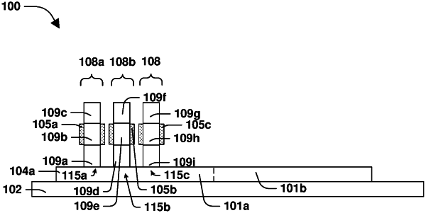
1. A method of forming a semiconductor arrangement, comprising:
forming a buffer layer;
forming a first dielectric layer over the buffer layer;
forming a first opening in the first dielectric layer, wherein the buffer layer is exposed through the first opening; and
forming a first semiconductor column in the first opening, wherein the first semiconductor column extends above a top surface of the first dielectric layer; and
removing the first dielectric layer after forming the first semiconductor column.
|