| CPC H01L 29/7816 (2013.01) [H01L 21/31111 (2013.01); H01L 21/32133 (2013.01); H01L 21/765 (2013.01); H01L 29/063 (2013.01); H01L 29/1095 (2013.01); H01L 29/402 (2013.01); H01L 29/408 (2013.01); H01L 29/66681 (2013.01); H01L 29/66795 (2013.01); H01L 29/7851 (2013.01)] | 18 Claims |

|
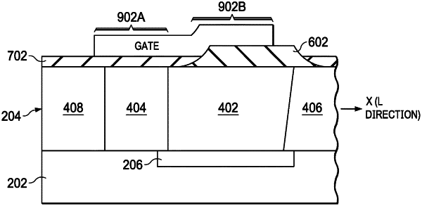
1. A method, comprising:
forming a fin on a substrate;
forming a field plating dielectric layer on a drift region of the fin;
forming a gate dielectric layer on a body region of the fin; and
forming a gate on the gate dielectric layer and a field plate on the field plating dielectric layer, the gate and the field plate forming a contiguous conductive layer.
|