| CPC H01L 29/7813 (2013.01) [H01L 21/266 (2013.01); H01L 29/407 (2013.01); H01L 29/41741 (2013.01); H01L 29/66712 (2013.01); H01L 29/7804 (2013.01)] | 4 Claims |
|
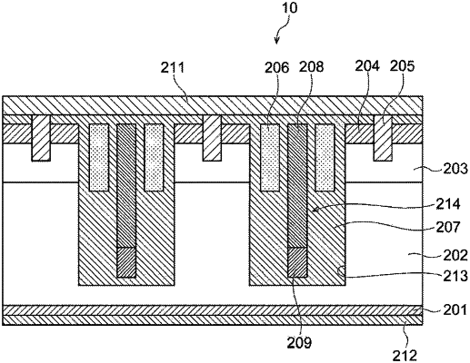
1. A semiconductor device manufacturing method, comprising:
forming a first semiconductor layer having a first conductive type at a main surface of a semiconductor substrate;
forming first opening portions at an interior of the first semiconductor layer;
forming an insulating film at bottom surface portions and side wall portions of the first opening portions, and forming concave portions;
forming first electrodes having the first conductive type at bottom surface portions of the concave portions;
forming second electrodes having a second conductive type at upper portions of the first electrodes, the second conductive type is a conductive type different from the first conductive type;
forming third electrodes at an interior of the insulating film;
forming a second semiconductor layer having the second conductive type at the first semiconductor layer at peripheries of the first opening portions; and
forming an impurity region having the first conductive type at an upper portion of the second semiconductor layer.
|