| CPC H01L 29/6625 (2013.01) [H01L 21/76895 (2013.01); H01L 23/535 (2013.01); H01L 29/0607 (2013.01); H01L 29/0653 (2013.01); H01L 29/66136 (2013.01); H01L 29/735 (2013.01); H01L 29/861 (2013.01); H02M 3/156 (2013.01)] | 20 Claims |

|
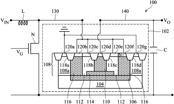
1. A method of making a triple well isolated diode comprising:
forming a buried layer in a substrate, wherein the buried layer has a second conductivity type and the substrate has a first conductivity type opposite to the second conductivity type;
forming an epi-layer over the substrate and the buried layer, wherein the epi-layer has the first conductivity type, and the epi-layer is part of the triple well isolated diode;
forming a first well in the epi-layer, wherein the first well has the second conductivity type;
forming a second well in the epi-layer, wherein the second well has the first conductivity type and surrounds the first well;
forming a third well in the epi-layer, wherein the third well has the second conductivity type and surrounds the second well, and a sidewall of the third well contacts a sidewall of the second well;
forming a deep well in the epi-layer, wherein the deep well has the first conductivity type and extends beneath the first well to electrically connect to the second well on both sides of the first well, and a portion of the second well lands directly on a top surface of the deep well;
forming a first plurality of isolation features between the first well and the second well; and
forming a second plurality of isolation features between the third well and a region of the epi-layer of the triple well isolated diode, wherein a first distance from a top surface of the substrate to a top-most surface of the region of the epi-layer of the triple well isolated diode is greater than a second distance from the top surface of the substrate to a bottommost surface of an isolation feature of the second plurality of isolation features.
|