| CPC H01L 29/0696 (2013.01) [G06F 30/39 (2020.01); H01L 29/0856 (2013.01); H01L 29/1045 (2013.01); H01L 29/105 (2013.01); H01L 29/42368 (2013.01); H01L 29/42376 (2013.01); H01L 29/4238 (2013.01); H01L 29/66068 (2013.01); H01L 29/7802 (2013.01); G06F 2119/08 (2020.01); H01L 29/1608 (2013.01)] | 20 Claims |

|
1. A semiconductor device comprising:
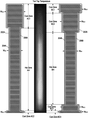
a first tub corresponding to a first region of a semiconductor die and including:
a first zone corresponding to a first projected operating temperature, and
a second zone corresponding to a second projected operating temperature greater than the first projected operating temperature,
wherein a first design parameter has a first value in the first zone and a second value different from the first value in the second zone,
wherein the first value being different from the second value configures the first tub to have a lower value for a first target operating parameter during operation of the semiconductor device than a value the first target operating parameter would have in a tub having a base tub design wherein the first value was equal to the second value, and
wherein the first target operating parameter is a maximum operating temperature in the second zone, a difference between a maximum operating temperature in the second zone and a maximum operating temperature in the first zone, a difference between a maximum operating temperature in the first tub and a minimum operating temperature in the first tub, or a combination thereof.
|