| CPC H01L 29/0634 (2013.01) [H01L 29/66712 (2013.01); H01L 29/7802 (2013.01)] | 12 Claims |

|
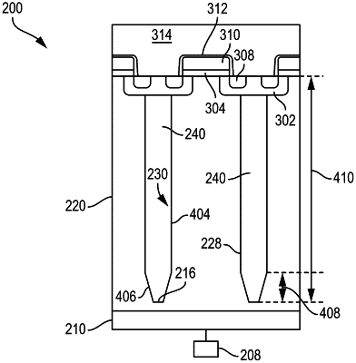
1. A method of processing a substrate, comprising:
depositing, via a first epitaxial growth process, an n-doped silicon material onto a substrate to form an n-doped layer while adjusting a ratio of dopant precursor to silicon precursor so that a dopant concentration of the n-doped layer increases from a bottom of the n-doped layer to a top of the n-doped layer;
etching the n-doped layer to form a plurality of trenches having sidewalls that are tapered and a plurality of n-doped pillars therebetween; and
filling the plurality of trenches with a p-doped material via a second epitaxial growth process to form a plurality of p-doped pillars, wherein at least one of:
the etching the n-doped layer further comprises etching a recess atop each of the plurality of trenches, wherein the recess is wider than the plurality of trenches, or
further comprising forming wells that are n-doped disposed atop or embedded within a top of each of the plurality of p-doped pillars.
|