| CPC H01L 27/1463 (2013.01) [H01L 27/14603 (2013.01); H01L 27/14621 (2013.01); H01L 27/14627 (2013.01); H01L 27/14636 (2013.01); H01L 27/14831 (2013.01)] | 20 Claims |

|
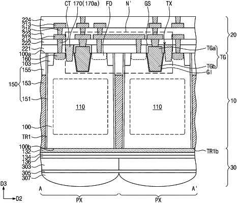
16. An image sensor, comprising:
a substrate having a first surface and a second surface, which are opposite to each other, the substrate comprising a pixel array region, an optical black region, and a pad region, the pixel array region comprising a plurality of unit pixel regions;
a pixel isolation pattern provided in the substrate to define the plurality of unit pixel regions, the pixel isolation pattern comprising an isolation filler pattern and an isolation liner interposed between the isolation filler pattern and the substrate;
a photoelectric conversion region provided in each of the plurality of unit pixel regions and adjacent to the second surface;
an impurity region and a floating diffusion region provided in each of the plurality of unit pixel regions and adjacent to the first surface;
a device isolation pattern provided on a side surface of the impurity region and a side surface of the floating diffusion region;
a gate electrode on the first surface of the substrate;
a gate dielectric layer interposed between the gate electrode and the substrate;
a gate spacer provided on top and side surfaces of the gate electrode;
an interconnection layer provided on the first surface of the substrate, the interconnection layer comprising an insulating layer and a plurality of interconnection lines in the insulating layer;
an auxiliary isolation pattern provided in the substrate and between the gate electrode and the impurity region and extended in a first direction, when the image sensor is viewed in a plan view;
an anti-reflection layer provided on the second surface of the substrate;
a back-side insulating layer on a bottom surface of the anti-reflection layer;
a color filter on a bottom surface of the back-side insulating layer; and
a micro lens on a bottom surface of the color filter,
wherein a bottom surface of the auxiliary isolation pattern is located at a level different from a bottom surface of the device isolation pattern.
|