| CPC H01L 27/1463 (2013.01) [H01L 27/1464 (2013.01); H01L 27/14685 (2013.01)] | 20 Claims |

|
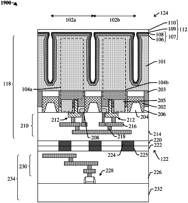
1. A method of forming an integrated chip, comprising:
forming a deep well comprising a first doping type into a substrate;
forming a plurality of deep trenches within the deep well to separate the deep well into a plurality of image sensing elements;
performing an etching process to remove an upper portion of the deep well exposed to the deep trenches and enlarge the deep trenches;
performing a low-temperature epitaxial growth process to form a first isolation epitaxial layer of the first doping type within the deep trenches and to form a second isolation epitaxial layer of a second doping type different than the first doping type over the first isolation epitaxial layer; and
filling remaining portions of the deep trenches with an isolation filler structure, wherein the first isolation epitaxial layer, the second isolation epitaxial layer, and the isolation filler structure form a backside deep trench isolation (BDTI) structure to isolate image sensing elements from one another,
wherein the first isolation epitaxial layer and the second isolation epitaxial layer are formed by forming a first isolation epitaxial precursor and a second isolation epitaxial precursor followed by performing a laser anneal process on the first isolation epitaxial precursor and the second isolation epitaxial precursor.
|