| CPC H01L 27/1462 (2013.01) [H01L 27/14618 (2013.01); H01L 27/14632 (2013.01); H01L 27/14636 (2013.01); H01L 27/14685 (2013.01); H01L 27/14687 (2013.01)] | 20 Claims |
|
1. A semiconductor packaging method, comprising:
providing a chip, wherein the chip includes:
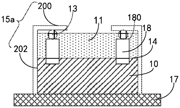
a chip substrate having a front surface and a back surface, wherein the front surface includes a photosensitive region;
soldering pads disposed at the front surface of the chip substrate surrounding the photosensitive region;
a metal part formed on a side of each soldering pad facing away from the chip substrate; and
a transparent protective layer formed on the front surface of the chip substrate, wherein the transparent protective layer covers the photosensitive region of the chip substrate the transparent protective layer encapsulates an entire sidewall of the metal part, and the transparent protective layer contains an opening at a position corresponding to the metal part to expose a first end of the metal part away from the soldering pads; and
electrically connecting the first end of the metal part to a circuit board using a conductive connection part to electrically connect the chip with the circuit board, the conductive connection part including:
a first portion electrically connecting to the first end of the metal part, the sidewall of the chip substrate being coplanar with the sidewall of the transparent protective layer, and
a second portion in parallel with the coplanar sidewalls of the chip substrate and the transparent protective layer.
|