| CPC H01L 27/14618 (2013.01) [G02B 1/041 (2013.01); G02B 1/11 (2013.01); H01L 27/1462 (2013.01); H01L 27/14621 (2013.01); H01L 27/14623 (2013.01); H01L 27/14627 (2013.01); H01L 27/1464 (2013.01); H01L 27/14645 (2013.01); H01L 27/14685 (2013.01)] | 8 Claims |

|
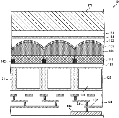
1. An imaging element, comprising:
a pixel on a semiconductor substrate;
a microlens adjacent to the pixel, wherein
the microlens is configured to:
collect incident light,
radiate the incident light on the pixel, and
flatten a surface of the pixel, and
the pixel is configured to generate an image signal based on the incident light radiated on the pixel;
a first transparent resin layer adjacent to the microlens,
wherein the first transparent resin layer has a refractive index different from a refractive index of the microlens by a difference of 0.4 to 0.6;
a first antireflection film;
a second antireflection film on a surface of the microlens,
wherein the first transparent resin layer is between the first antireflection film and the second antireflection film; and
a sealing glass adjacent to the first transparent resin layer,
wherein the sealing glass seals the semiconductor substrate.
|