| CPC H01L 27/14612 (2013.01) [H01L 27/14636 (2013.01); H04N 25/75 (2023.01); H04N 25/77 (2023.01)] | 12 Claims |

|
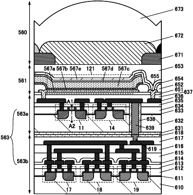
1. An imaging device comprising a plurality of pixel blocks, wherein each of the plurality of pixel blocks comprises N first circuits, N second circuits, a third circuit, and a wiring electrically connected to the third circuit,
wherein N is an integer greater than or equal to 1,
wherein each of the N first circuits comprises a photoelectric conversion device,
wherein the photoelectric conversion device is configured to convert incident light into an electrical signal,
wherein the K-th first circuit is configured to output a first signal that is obtained by binarizing the electrical signal to the K-th second circuit via a first transistor provided in the K-th first circuit,
wherein K is an integer greater than or equal to 1 and less than or equal to N,
wherein each of the N second circuits is configured to generate a second signal by multiplying the first signal by a weight coefficient and output the second signal to the wiring,
wherein the N second signals are added by being output to the wiring,
wherein one of a source and a drain of the first transistor is electrically connected to a first terminal of a fourth circuit provided in the K-th second circuit, and
wherein the other of the source and the drain of the first transistor is electrically connected to a first switch provided in the K-th second circuit.
|