| CPC H01L 27/1255 (2013.01) [H01L 27/124 (2013.01); H01L 27/1259 (2013.01); H01L 29/78648 (2013.01)] | 18 Claims |

|
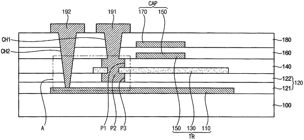
1. A method of manufacturing a display substrate, the method comprising:
forming a first gate electrode on a substrate;
forming a first gate insulating layer on the substrate to cover the first gate electrode;
forming an active layer on the first gate insulating layer, the active layer comprising a source region, a channel region, and a drain region;
forming a second gate insulating layer on the first gate insulating layer to cover the active layer;
forming a second gate electrode on the second gate insulating layer;
forming an interlayer insulating layer on the second gate insulating layer to cover the second gate electrode;
forming a first contact hole through the interlayer insulating layer, the second gate insulating layer, the active layer, and a portion of the first gate insulating layer to expose a top surface, a side wall, and a bottom surface of the active layer;
forming a second contact hole spaced from the active layer and through the interlayer insulating layer, the second gate insulating layer, and the first gate insulating layer to expose the first gate electrode; and
forming a first electrode to fill the first contact hole and a second electrode to fill the second contact hole on the interlayer insulating layer,
wherein the first contact hole and the second contact hole are concurrently formed.
|