| CPC H01L 27/1248 (2013.01) [H01L 27/1259 (2013.01)] | 14 Claims |

|
1. An array substrate, comprising:
a substrate;
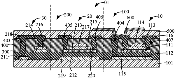
a switching transistor and a driving transistor disposed on the substrate, wherein an orthogonal projection of the switching transistor on the substrate is staggered from an orthogonal projection of the driving transistor on the substrate,
a mobility of the switching transistor is greater than a mobility of the driving transistor, and a threshold voltage of the driving transistor is less than a threshold voltage of the switching transistor,
wherein the switching transistor comprises a first gate electrode and a second gate electrode connected to the first gate electrode, and the driving transistor comprises a first oxide semiconductor portion, wherein the first oxide semiconductor portion is doped with one or a combination of two of electronegative metal and an electronegative compound,
wherein the driving transistor and the switching transistor are both disposed in a same layer on the substrate, and the substrate comprises a display area and a non-display area disposed adjacent to each other, wherein the driving transistor is located in the display area, and the switching transistor is located in the non-display area, and
wherein the non-display area comprises a bridge area and a main area that are disposed adjacent to each other, wherein the bridge area is located on a side of the main area away from the display area; the first gate electrode comprises a first sub-gate electrode and a first light-shielding portion spaced apart from each other, wherein the first sub-gate electrode is located in the bridge area of the substrate, and the first light-shielding portion is located in the main area of the substrate; and the second gate electrode comprises a second sub-gate electrode and a third sub-gate electrode spaced apart from each other, wherein the second sub-gate electrode is located in the bridge area and above the first sub-gate electrode, the first sub-gate electrode is connected to the second sub-gate electrode, and the third sub-gate electrode is located in the main area and above the first light-shielding portion.
|