| CPC H01L 27/1218 (2013.01) [H01L 25/162 (2013.01); H01L 25/167 (2013.01); H01L 27/124 (2013.01)] | 23 Claims |

|
1. A tiled display device comprising:
a plurality of display devices comprising a plurality of display areas comprising a plurality of pixels, and a coupling area between adjacent display areas from among the plurality of display areas,
wherein each of the plurality of display devices comprises:
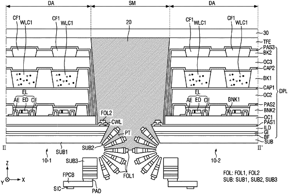
a substrate comprising a first portion configured to support the display area, a second portion extending from the first portion to be bent, and a third portion extending from the second portion;
a thin film transistor layer on the first portion, the second portion, and the third portion of the substrate and comprising a thin film transistor;
a display layer comprising the thin film transistor on the first portion of the substrate, and the plurality of pixels;
a connection line at an edge of the first portion of the substrate and connected to the plurality of pixels;
a pad portion on the third portion of the substrate;
a fan-out line on the second portion of the substrate and connected between the pad portion and the connection line; and
a plurality of pattern holes penetrating the thin film transistor layer and the second portion of the substrate.
|