| CPC H01L 27/0924 (2013.01) [H01L 21/823821 (2013.01); H01L 21/823871 (2013.01); H01L 23/5286 (2013.01)] | 20 Claims |

|
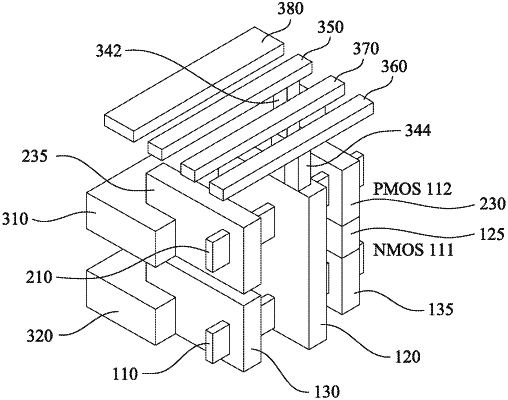
1. A semiconductor device having a standard cell, the standard cell comprising:
a first gate-all-around field effect transistor (GAA FET) disposed over a substrate;
a second GAA FET disposed at a vertically different level from the first GAA FET and sharing a gate with the first GAA FET;
a first power supply line;
a second power supply line; and
a first signal line, a second signal line, a third signal line and a fourth signal line, which are disposed above the first GAA FET and the second GAA FET, wherein:
the first, second, third and fourth signal lines are located at a same level with each other,
the first power supply line and the second power supply line are located at vertically different levels from each other, and
a cell height of the standard cell is 4 T, where T is a pitch between the first and second signal lines, the second and third signal lines, and the third and fourth signal lines in plan view.
|