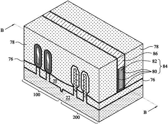
| CPC H01L 27/0924 (2013.01) [H01L 21/02532 (2013.01); H01L 21/02636 (2013.01); H01L 21/30604 (2013.01); H01L 21/3081 (2013.01); H01L 21/31111 (2013.01); H01L 21/76224 (2013.01); H01L 21/76229 (2013.01); H01L 21/823821 (2013.01); H01L 21/845 (2013.01); H01L 27/0922 (2013.01); H01L 27/1207 (2013.01); H01L 27/1211 (2013.01); H01L 29/0649 (2013.01); H01L 29/6653 (2013.01); H01L 29/66545 (2013.01); H01L 21/30625 (2013.01); H01L 21/823807 (2013.01); H01L 21/823828 (2013.01); H01L 29/045 (2013.01); H01L 29/165 (2013.01); H01L 29/7848 (2013.01)] | 20 Claims |

|
1. A method comprising:
etching a semiconductor substrate to form:
a first semiconductor strip in a first device region, wherein the first semiconductor strip has a first top surface crystal orientation; and
a second semiconductor strip in a second device region; and
forming an isolation region comprising:
a bulk portion comprising a first sidewall contacting the first semiconductor strip, and a second sidewall contacting the second semiconductor strip; and
a protruding portion protruding from a bottom surface of the bulk portion downwardly to a level lower than bottoms of the first semiconductor strip and the second semiconductor strip, wherein the protruding portion recesses laterally from the first sidewall and the second sidewall toward a first middle line between the first sidewall and the second sidewall; and
forming a source/drain region overlapping the first semiconductor strip, wherein the source/drain region comprises:
a lower portion having the first top surface crystal orientation; and
an upper portion over the lower portion, wherein the upper portion has a second top surface crystal orientation different from the first top surface crystal orientation.
|