| CPC H01L 27/0924 (2013.01) [H01L 21/823431 (2013.01); H01L 21/823468 (2013.01); H01L 29/0649 (2013.01); H01L 29/0847 (2013.01); H01L 29/6656 (2013.01); H01L 29/66795 (2013.01); H01L 29/7851 (2013.01)] | 20 Claims |
|
1. A device comprising:
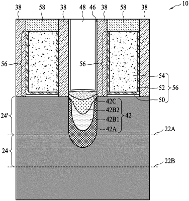
a semiconductor substrate;
isolation regions extending into the semiconductor substrate;
a semiconductor fin between the isolation regions, wherein the semiconductor fin protrudes higher than top surfaces of the isolation regions;
a gate stack on a top surface and sidewalls of the semiconductor fin; and
an epitaxy source/drain region on a side of the semiconductor fin, wherein the epitaxy source/drain region extends to a level lower than top surfaces of the isolation regions, and wherein the epitaxy source/drain region comprises:
a first semiconductor layer having a first dopant concentration; and
an embedded stressor over and contacting the first semiconductor layer, wherein the embedded stressor has a second dopant concentration higher than the first dopant concentration, and wherein the embedded stressor has an upper portion higher than the top surface of the semiconductor fin, and a lower portion lower than the top surface of the semiconductor fin.
|