| CPC H01L 27/0886 (2013.01) [H01L 21/02181 (2013.01); H01L 21/31144 (2013.01); H01L 21/32133 (2013.01); H01L 21/76802 (2013.01); H01L 21/76877 (2013.01); H01L 21/823431 (2013.01); H01L 21/823437 (2013.01); H01L 21/823468 (2013.01); H01L 21/823475 (2013.01); H01L 21/823821 (2013.01); H01L 23/5286 (2013.01); H01L 23/5329 (2013.01); H01L 23/62 (2013.01); H01L 27/0924 (2013.01); H01L 29/66545 (2013.01); H01L 29/66795 (2013.01); H01L 29/785 (2013.01)] | 20 Claims |

|
1. A semiconductor structure comprising:
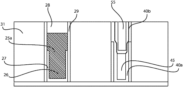
a first gate structure and a second gate structure in-line with one another and separated by a gate cut; and
a trench comprising a power rail, wherein:
the first and second gate structures extend in a first horizontal direction and each comprise a metal gate and a dielectric gate cap;
the trench and the power rail extend through the gate cut in a second horizontal direction perpendicular to the first horizontal direction; and
an upper surface of the dielectric gate cap of the first gate structure is substantially co-planar with an upper surface of the power rail.
|