| CPC H01L 27/0886 (2013.01) [H01L 21/02164 (2013.01); H01L 21/0217 (2013.01); H01L 21/022 (2013.01); H01L 21/0228 (2013.01); H01L 21/823431 (2013.01); H01L 21/823437 (2013.01); H01L 21/823481 (2013.01); H01L 29/0649 (2013.01); H01L 29/66545 (2013.01); H01L 29/66795 (2013.01); H01L 29/785 (2013.01)] | 10 Claims |

|
1. A semiconductor structure, comprising:
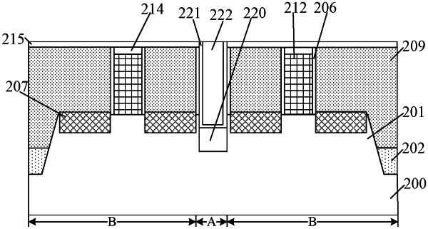
a substrate including device regions and an isolation region located adjacent to and between the device regions;
a fin on the substrate;
gate structures across the fin at the device regions;
source/drain doped regions in the fin at two sides of each of the gate structures;
a first opening in the fin at the isolation region;
an insulation structure located in the first opening, the insulation structure including a first insulation layer at a bottom of the first opening, a second insulation layer on a top surface of the first insulation layer and sidewall surfaces of the first opening, and a third insulation layer on a top surface and sidewall surfaces of the second insulation layer, the first insulation layer and the third insulation layer being made of a first material, and the second insulation layer being made of a second material different from the first material;
isolation structures disposed at the device region and on a top surface of the substrate at two sides of the fin, top surfaces of the isolation structures being lower than a top surface of the fin, and the isolation structures covering a portion of sidewalls of the fin; and
a first dielectric layer on top surfaces of the source/drain doped regions, the sidewalls and the top surface of the fin, the top surfaces of the isolation structures, and sidewalls of the gate structures;
wherein:
two opposite sidewalls of the first opening are respectively in contact with the source/drain doped regions at adjacent device regions;
a top surface of the insulation structure is flush with or higher than the top surfaces of the source/drain doped regions;
a top surface of the third insulation layer is higher than top surface of the first dielectric layer, and the top surfaces of the first dielectric layer are higher than top surfaces of the gate structures;
the top surface of the first insulation layer is higher than bottom surfaces of the source/drain doped regions and is lower than the top surfaces of the source/drain doped regions, and a thickness of the first insulation layer along a vertical direction is uniform; and
the top surface of the first insulation layer is higher than the top surfaces of the isolation structures, and a bottom surface of the first insulation layer is higher than bottom surfaces of the isolation structures.
|