US 12,074,162 B2
Structure and formation method of semiconductor device with capacitors
Guo-Jyun Luo, Taipei (TW); Chen-Chien Chang, Zhubei (TW); Chiu-Hua Chung, Hsinchu (TW); Shiuan-Jeng Lin, Hsinchu (TW); and Han-Zong Pan, Hsinchu (TW)
Assigned to Taiwan Semiconductor Manufacturing Company, Ltd., Hsinchu (TW)
Filed by Taiwan Semiconductor Manufacturing Company, Ltd., Hsin-Chu (TW)
Filed on Jun. 17, 2021, as Appl. No. 17/350,349.
Application 17/350,349 is a continuation of application No. 16/991,385, filed on Aug. 12, 2020.
Application 16/991,385 is a continuation of application No. 15/940,075, filed on Mar. 29, 2018, granted, now 10,748,986, issued on Aug. 18, 2020.
Claims priority of provisional application 62/589,289, filed on Nov. 21, 2017.
Prior Publication US 2021/0313416 A1, Oct. 7, 2021
Int. Cl. H01L 27/08 (2006.01); H01L 21/285 (2006.01); H01L 27/06 (2006.01); H01L 49/02 (2006.01)
CPC H01L 27/0805 (2013.01) [H01L 21/2855 (2013.01); H01L 27/0629 (2013.01); H01L 28/40 (2013.01)] 20 Claims
OG exemplary drawing
 
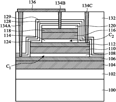
1. A semiconductor structure, comprising:
a lower electrode over a substrate;
a first capacitor dielectric layer over the lower electrode;
an intermediate electrode over the first capacitor dielectric layer;
a second capacitor dielectric layer over the intermediate electrode;
an upper electrode over the second capacitor dielectric layer, wherein the upper electrode is completely confined over the intermediate electrode; and
a first protection layer completely confined over the intermediate electrode, wherein the first protection layer covers opposing sidewalls of the upper electrode and upper surfaces of the intermediate electrode and the upper electrode.