| CPC H01L 27/0266 (2013.01) [H01L 21/02293 (2013.01); H01L 27/0248 (2013.01); H01L 27/0886 (2013.01); H01L 29/0847 (2013.01); H01L 29/1608 (2013.01); H01L 29/7831 (2013.01); H01L 29/785 (2013.01)] | 10 Claims |

|
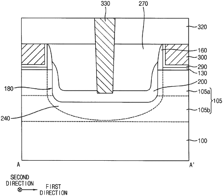
1. A method of manufacturing an electrostatic discharge (ESD) protection device, the method comprising:
forming a plurality of gate structures on a substrate, the substrate including an active fin extending in a first direction, and each gate structure of the plurality of gate structures extending in a second direction subtending an angle with the first direction and covering a respective part of the active fin;
forming a recess on a portion of the active fin between gate structures;
forming an epitaxial layer on the recess;
implanting impurities into the epitaxial layer and the active fin to form an impurity region at a portion of the active fin under the epitaxial layer; and
forming a contact plug contacting a top of the epitaxial layer,
wherein:
a central portion of the impurity region in the first direction has a thickness in a vertical direction substantially perpendicular to an upper surface of the substrate that is greater than a thickness in the vertical direction of an edge portion of the impurity region located to a side of the central portion in the first direction, the central portion and the edge portion of the impurity region entirely underlying the epitaxial layer, and a lowermost surface of the central portion of the impurity region being lower than a lowermost surface of the edge portion of the impurity region,
a top of a central portion of the epitaxial layer is disposed at a level beneath that of an edge portion of the epitaxial layer in the first direction, and
the contact plug overlaps the central portion of the impurity region in the vertical direction.
|