| CPC H01L 25/16 (2013.01) [H01L 23/367 (2013.01); H01L 23/66 (2013.01); H01L 24/48 (2013.01); H01L 2223/6655 (2013.01); H01L 2224/48137 (2013.01); H01L 2224/48175 (2013.01); H01L 2924/1033 (2013.01); H01L 2924/13064 (2013.01); H01L 2924/1421 (2013.01); H01L 2924/19105 (2013.01); H01L 2924/30111 (2013.01)] | 19 Claims |
|
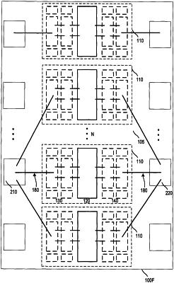
1. A semiconductor device package comprising:
a first and a second input lead;
a first and a second output lead; and
a plurality of uniform transistor-based components, the plurality of uniform transistor-based components comprising a first subset including one or more first uniform transistor-based components coupled to the first input lead, and a second subset including one or more second uniform transistor-based components coupled to the second input lead,
wherein the first input lead and the first output lead define a first amplifier path therebetween,
wherein the second input lead and the second output lead define a second amplifier path therebetween,
wherein the first amplifier path and the second amplifier path are asymmetric with respect to one another, and
wherein each of the one or more first and second uniform transistor-based components respectively comprises a same matching device that is distinct from a transistor thereof and includes a first integrated passive device (IPD) circuit, wherein the first IPD circuit comprises a main element and a tunable element that is configured to be selectively connected to the main element to alter an impedance of the first IPD circuit to provide one of a first impedance and a second impedance that is different from the first impedance.
|