| CPC H01L 25/075 (2013.01) [H01L 2933/0033 (2013.01); H01L 2933/005 (2013.01); H01L 2933/0066 (2013.01)] | 20 Claims |

|
1. A display device, comprising:
a substrate extending along a first direction and having a plurality of first substrate electrodes and a plurality of second substrate electrodes; and
a plurality of light sources disposed on the substrate and spaced apart from one another,
wherein the light source comprises:
a light emitting layer having an n-type semiconductor layer, an active layer, and a p-type semiconductor layer;
a p-type electrode disposed on the p-type semiconductor layer and electrically connected to the p-type semiconductor layer; and
an n-type electrode disposed on the n-type semiconductor layer and electrically connected to the n-type semiconductor layer,
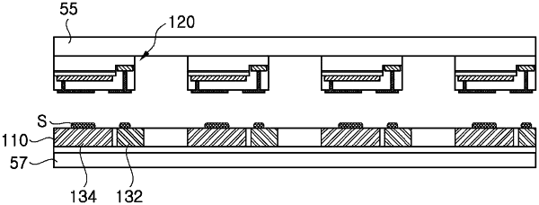
wherein at least one of the first substrate electrodes includes an upper side comprising a substantially flat region and a lower side comprising a substantially flat region disposed on the substrate, the first substrate electrode is electrically connected to the p-type electrode,
wherein at least one of the second substrate electrodes includes an upper side comprising a substantially flat region and a lower side comprising a substantially flat region disposed on the substrate, the second substrate electrode is electrically connected to the n-type electrode,
wherein at least one upper side of the plurality of first substrate electrodes is electrically connected to a first light source and at least one upper side of the plurality of second substrate electrodes is electrically connected to a second light source adjacent to the first light source, the first light source and the second light source are spaced apart from each other, and
wherein a width of the upper side of the first substrate electrode in the first direction is greater than that of the p-type electrode, and a width of the upper side of the second substrate electrode in the first direction is greater than that of the n-type electrode.
|