| CPC H01L 25/0657 (2013.01) [H01L 23/3157 (2013.01); H01L 23/481 (2013.01); H01L 24/16 (2013.01); H01L 24/17 (2013.01); H01L 24/73 (2013.01); H01L 24/81 (2013.01); H01L 25/50 (2013.01); H01L 2224/16146 (2013.01); H01L 2224/17177 (2013.01); H01L 2224/73204 (2013.01); H01L 2224/81203 (2013.01)] | 20 Claims |

|
1. A semiconductor package, comprising:
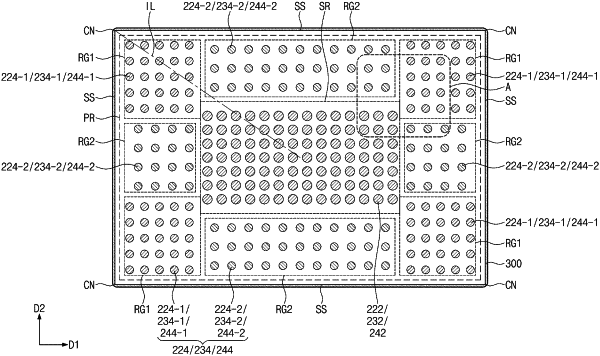
a first die having a signal region and a peripheral region that surrounds the signal region, the first die including a plurality of first vias on the peripheral region;
a second die on the first die and having a plurality of second vias on the peripheral region, the plurality of second vias being on positions that correspond to positions of the first vias; and
a plurality of connection terminals between the first die and the second die, the plurality of connection terminals connecting the plurality of second vias to the plurality of first vias,
wherein the peripheral region includes a plurality of first regions and a plurality of second regions,
the plurality of first regions are adjacent to corners of the first die when viewed in a plan view, and
the plurality of second regions are adjacent to lateral surfaces of the first die when viewed in the plan view,
wherein the plurality of connection terminals include a plurality of first connection terminals on the plurality of first regions and a plurality of second connection terminals on the plurality of second regions, and
wherein a sum of areas of the plurality of first connection terminals per unit area on the plurality of first regions is greater than a sum of areas of the plurality of second connection terminals per unit area on the plurality of second regions.
|