| CPC H01L 25/0655 (2013.01) [H01L 23/5226 (2013.01); H01L 23/5384 (2013.01); H01L 24/13 (2013.01); H01L 2225/06541 (2013.01)] | 20 Claims |
|
1. An integrated circuit assembly, comprising:
a first integrated circuit die comprising:
a first substrate;
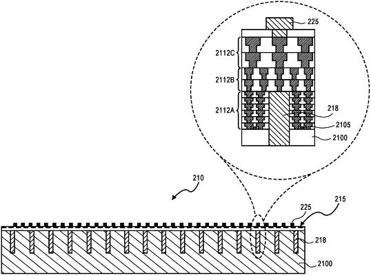
a device region on the first substrate including a plurality of transistor devices;
a first interconnect level over the device region;
a second interconnect level over the first interconnect level;
a third interconnect level over the second interconnect level;
a device contact point over the third interconnect level;
a backside contact at an opposite side of the first substrate than the device region;
a through silicon via (TSV), the TSV extending from the backside contact through the first substrate to a location between the first interconnect level and the third interconnect level; and
wherein the first integrated circuit die has a footprint; and
a second integrated circuit die comprising:
a second substrate;
a second device region on the second substrate;
a device side including a device contact point thereon;
a backside opposite the device side; and
wherein the second integrated circuit die is located over the first integrated circuit die, and wherein the device contact point of the second integrated circuit die is coupled to the device contact point of the first integrated circuit die, and wherein the second integrated circuit die has a footprint within the footprint of the first integrated circuit die.
|