US 12,074,136 B2
Package structure and method of manufacturing the same
Tzuan-Horng Liu, Taoyuan (TW); Hsien-Wei Chen, Hsinchu (TW); Jiun-Heng Wang, Hsinchu County (TW); and Ming-Fa Chen, Taichung (TW)
Assigned to Taiwan Semiconductor Manufacturing Company, Ltd., Hsinchu (TW)
Filed by Taiwan Semiconductor Manufacturing Company, Ltd., Hsinchu (TW)
Filed on Feb. 5, 2023, as Appl. No. 18/164,607.
Application 18/164,607 is a continuation of application No. 17/200,906, filed on Mar. 15, 2021, granted, now 11,587,907.
Application 17/200,906 is a continuation of application No. 16/655,266, filed on Oct. 17, 2019, granted, now 10,950,576, issued on Mar. 16, 2021.
Application 16/655,266 is a continuation of application No. 15/980,676, filed on May 15, 2018, granted, now 10,468,379, issued on Nov. 5, 2019.
Prior Publication US 2023/0178516 A1, Jun. 8, 2023
Int. Cl. H01L 25/00 (2006.01); H01L 21/66 (2006.01); H01L 23/00 (2006.01); H01L 23/498 (2006.01); H01L 23/522 (2006.01); H01L 25/065 (2023.01)
CPC H01L 25/0652 (2013.01) [H01L 22/32 (2013.01); H01L 23/49827 (2013.01); H01L 23/5226 (2013.01); H01L 24/09 (2013.01); H01L 24/32 (2013.01); H01L 24/83 (2013.01); H01L 25/50 (2013.01); H01L 2224/02372 (2013.01)] 20 Claims
OG exemplary drawing
 
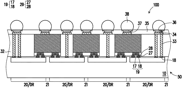
1. A package structure, comprising:
a plurality of first dies on first regions of a semiconductor substrate; and
a plurality of second dies electrically bonded to the plurality of first dies;
wherein the plurality of second dies cover a second region of the semiconductor substrate between the first regions of the semiconductor substrate,
wherein first portions of top surfaces of the plurality of first dies are covered by the plurality of second dies, and second portions of the top surfaces of the plurality of first dies are exposed by the plurality of second dies,
wherein the plurality of first dies are connected to the semiconductor substrate, and sandwiched between the semiconductor substrate and the plurality of second dies.