| CPC H01L 24/94 (2013.01) [H01L 21/563 (2013.01); H01L 21/565 (2013.01); H01L 23/3171 (2013.01); H01L 23/49816 (2013.01); H01L 23/49822 (2013.01); H01L 24/11 (2013.01); H01L 24/16 (2013.01); H01L 25/0657 (2013.01); H01L 24/95 (2013.01); H01L 2224/10126 (2013.01); H01L 2224/10145 (2013.01); H01L 2224/11849 (2013.01); H01L 2224/16146 (2013.01); H01L 2225/06513 (2013.01); H01L 2924/182 (2013.01)] | 19 Claims |

|
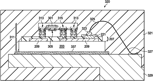
1. An apparatus, comprising:
a first semiconductor die with a component on a first surface, the first semiconductor die having an opposite second surface;
a second semiconductor die mounted on a package substrate and having a third surface facing away from the package substrate;
a solder seal bonded to and extending from the first surface of the first semiconductor die which is flip chip mounted to the third surface of the second semiconductor die, the solder seal at least partially surrounding the component;
a first solder joint formed between the solder seal and a dielectric material overlying the third surface of the second semiconductor die, the first solder joint physically contacting the dielectric material;
a post connect extending from the first surface of the first semiconductor die;
a second solder joint formed between solder at an end of the post connect and a conductive land on a dielectric layer overlying the third surface of the second semiconductor die; and
a mold compound covering the second surface of the first semiconductor die, a portion of the second semiconductor die, and an outside periphery of the solder seal.
|