| CPC H01L 24/48 (2013.01) [H01L 23/12 (2013.01); H01L 23/3121 (2013.01); H01L 23/3675 (2013.01); H01L 24/05 (2013.01); H01L 24/06 (2013.01); H01L 2224/05101 (2013.01); H01L 2224/0603 (2013.01); H01L 2224/4813 (2013.01); H01L 2224/4846 (2013.01)] | 8 Claims |

|
1. A semiconductor device comprising:
a first circuit;
a second circuit;
a wiring member connected to one of the first circuit and the second circuit;
a bonding material connected to the other of the first circuit and the second circuit; and
a semiconductor element,
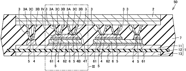
the wiring member including a first end, a second end, and a top, the first end and the second end being connected to one of the first circuit and the second circuit, the top being located between the first end and the second end,
the top being connected to the other of the first circuit and the second circuit with the bonding material in between,
the semiconductor element including a pad,
the bonding material being disposed on the pad of the semiconductor element,
the first end and the second end being directly joined to the second circuit,
the top being connected to the first circuit with the bonding material and the semiconductor element in between.
|