| CPC H01L 24/05 (2013.01) [H01L 23/48 (2013.01); H01L 23/481 (2013.01); H01L 23/482 (2013.01); H01L 23/4824 (2013.01); H01L 23/485 (2013.01); H01L 23/49811 (2013.01); H01L 23/49838 (2013.01); H01L 23/52 (2013.01); H01L 23/522 (2013.01); H01L 23/5226 (2013.01); H01L 23/528 (2013.01); H01L 23/5329 (2013.01); H01L 24/10 (2013.01); H01L 24/11 (2013.01); H01L 24/12 (2013.01); H01L 24/13 (2013.01); H01L 24/26 (2013.01); H01L 24/28 (2013.01); H01L 24/29 (2013.01); H01L 23/53228 (2013.01); H01L 2224/0225 (2013.01); H01L 2224/0226 (2013.01); H01L 2224/0401 (2013.01); H01L 2224/05124 (2013.01); H01L 2224/05147 (2013.01); H01L 2224/05166 (2013.01); H01L 2224/05171 (2013.01); H01L 2224/05184 (2013.01); H01L 2224/05644 (2013.01); H01L 2224/05647 (2013.01); H01L 2224/05655 (2013.01); H01L 2224/05666 (2013.01); H01L 2224/11464 (2013.01); H01L 2224/1147 (2013.01); H01L 2224/13 (2013.01); H01L 2224/13018 (2013.01); H01L 2224/13026 (2013.01); H01L 2224/13082 (2013.01); H01L 2224/13099 (2013.01); H01L 2224/13147 (2013.01); H01L 2224/13155 (2013.01); H01L 2224/16 (2013.01); H01L 2924/01006 (2013.01); H01L 2924/01013 (2013.01); H01L 2924/01019 (2013.01); H01L 2924/01022 (2013.01); H01L 2924/01024 (2013.01); H01L 2924/01029 (2013.01); H01L 2924/01032 (2013.01); H01L 2924/01033 (2013.01); H01L 2924/01046 (2013.01); H01L 2924/01047 (2013.01); H01L 2924/0105 (2013.01); H01L 2924/01073 (2013.01); H01L 2924/01074 (2013.01); H01L 2924/01075 (2013.01); H01L 2924/01078 (2013.01); H01L 2924/01079 (2013.01); H01L 2924/01082 (2013.01); H01L 2924/014 (2013.01); H01L 2924/07025 (2013.01); H01L 2924/19041 (2013.01); H01L 2924/35121 (2013.01)] | 20 Claims |
|
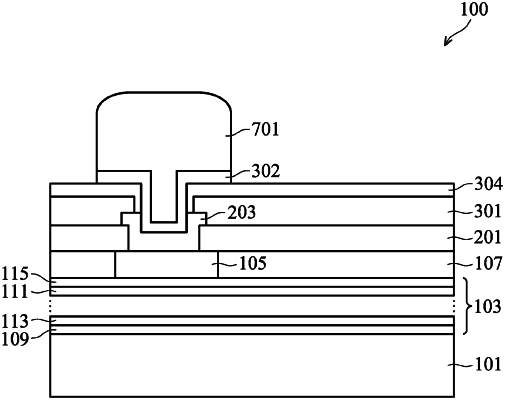
1. A semiconductor device comprising:
a conductive feature over a substrate, the conductive feature having a thickness of at least 15,000 Å;
a contact making physical contact with the conductive feature, the contact having a smaller width than the conductive feature, the contact comprising a U-shape in a cross-sectional view; and
a conductive pillar extending below a top surface of the contact.
|