| CPC H01L 23/66 (2013.01) [H01L 23/49816 (2013.01); H01L 23/49827 (2013.01); H01L 23/49833 (2013.01); H01L 23/49838 (2013.01); H01L 23/5225 (2013.01); H01L 23/552 (2013.01); H01L 24/17 (2013.01); H01L 25/0657 (2013.01); H01L 25/18 (2013.01); H01L 2223/6622 (2013.01); H01L 2223/6638 (2013.01); H01L 2224/16225 (2013.01); H01L 2924/141 (2013.01); H01L 2924/1421 (2013.01); H01L 2924/1432 (2013.01); H01L 2924/1434 (2013.01); H01L 2924/1436 (2013.01); H01L 2924/1443 (2013.01); H01L 2924/146 (2013.01); H01L 2924/3025 (2013.01)] | 20 Claims |

|
1. A semiconductor package, comprising:
a first semiconductor device;
a second semiconductor device including a continuous ground shielding;
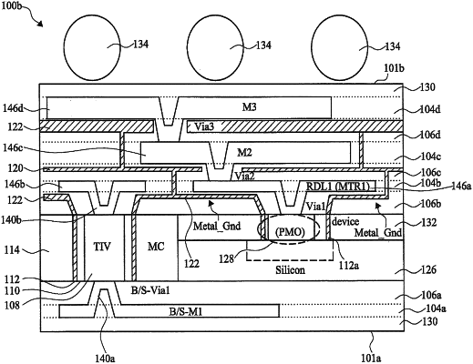
a ground shielded transmission path coupling the first semiconductor device to the second semiconductor device, the ground shielded transmission path comprising:
at least one signal path extending longitudinally between a first end and a second end, the at least one signal path including an electrically conductive material;
a first insulating layer disposed over the at least one signal path longitudinally between the first end and the second end, wherein the first insulating layer includes an electrically insulating material; and
a ground shielding layer disposed over the electrically insulating material longitudinally between the first end and the second end of the at least one signal path, wherein the ground shielding layer includes an electrically conductive material, and wherein each of the continuous ground shielding and the ground shielding layer are coupled to ground,
wherein the at least one signal path comprises a quadrantal signal path including a first transmission path, a second transmission path, a third transmission path, and a fourth transmission path.
|