| CPC H01L 23/66 (2013.01) [H01L 23/3107 (2013.01); H01L 23/49811 (2013.01); H01L 23/49822 (2013.01); H01L 23/552 (2013.01); H01Q 9/0407 (2013.01); H05K 1/0237 (2013.01); H01L 2223/6627 (2013.01); H05K 2201/10098 (2013.01)] | 17 Claims |

|
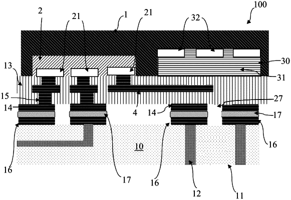
1. An integrated circuit package comprising:
an encapsulant;
a semiconductor die in the encapsulant, the semiconductor die comprising a plurality of die terminals;
an integrated waveguide launcher, wherein the integrated waveguide launcher is connected to one of the die terminals; and
a land grid array provided on a bottom surface of the package, the land grid array comprising:
a plurality of package terminals, each package terminal configured to be soldered to a connection;
a metal pad substantially surrounded by the plurality of package terminals; and
an opening formed in the metal pad, wherein the opening is aligned with the integrated waveguide launcher.
|