| CPC H01L 23/5389 (2013.01) [H01L 23/367 (2013.01); H01L 25/072 (2013.01); H01L 25/16 (2013.01); H01L 25/18 (2013.01)] | 12 Claims |
|
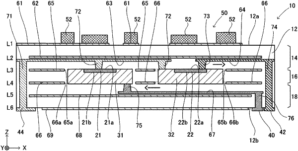
1. A semiconductor device comprising:
a substrate main body having a first surface and a second surface;
an electric component arranged in the substrate main body;
a first terminal and a second terminal both arranged on one of the first surface and the second surface;
a first internal conductor pattern arranged in a first circuit layer arranged between the electric component and the first surface, and electrically connected to the first terminal and the electric component; and
a second internal conductor pattern arranged in a second circuit layer arranged between the electric component and the second surface, and electrically connected to the second terminal and the electric component, wherein:
the first internal conductor pattern and the second internal conductor pattern are at least partially opposed to each other inside the substrate main body,
the electric component includes a first semiconductor element and a second semiconductor element, each of the first semiconductor element and the second semiconductor element including a power semiconductor element and a heat sink plate to which the power semiconductor element is bonded,
each heat sink plate is arranged in the substrate main body and is in contact with its corresponding bonded power semiconductor element
the first semiconductor element and the second semiconductor element are arranged side by side, both disposed between the first internal conductor pattern and the second internal conductor pattern in a stacking direction, and
a current path of the first internal conductor pattern is in parallel and opposite to a current path of the second internal conductor pattern.
|