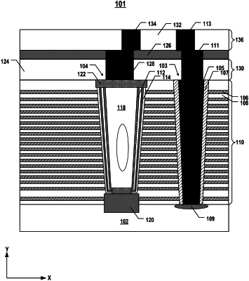
| CPC H01L 23/5226 (2013.01) [H01L 23/5283 (2013.01); H10B 43/27 (2023.02); H10B 43/35 (2023.02)] | 20 Claims |

|
1. A three-dimensional (3D) memory device, comprising:
a memory stack comprising interleaved conductive layers and dielectric layers;
a channel structure extending vertically through the memory stack, an upper end of a plug of the channel structure being coplanar with an upper surface of the memory stack;
a first dielectric layer having a first dielectric material in contact with the memory stack and the plug;
an intermedia dielectric layer on the first dielectric layer and having a second dielectric material different from the first dielectric material;
a second dielectric layer on the intermedia dielectric layer;
a slit structure extending along a lateral direction to separate the memory stack, and comprising a lower portion having polysilicon and an upper portion having metal;
a first contact penetrating the intermedia dielectric layer and the first dielectric layer, the first contact being in contact with the plug of the channel structure, a first lateral dimension of an upper end of the first contact is not less than a second lateral dimension of a lower end of the first contact;
a second contact penetrating the second dielectric layer and in contact with at least the upper end of the first contact;
a third contact penetrating the intermedia dielectric layer and the first dielectric layer, the third contact being in contact with the upper portion of the slit structure; and
a fourth contact penetrating the second dielectric layer and in contact with at least the upper end of the third contact.
|