| CPC H01L 23/5226 (2013.01) [H01L 21/56 (2013.01); H01L 21/563 (2013.01); H01L 21/76871 (2013.01); H01L 21/76877 (2013.01); H01L 23/3121 (2013.01); H01L 23/49827 (2013.01); H01L 24/09 (2013.01); H01L 24/14 (2013.01); H01L 2224/02372 (2013.01); H01L 2224/0401 (2013.01)] | 20 Claims |
|
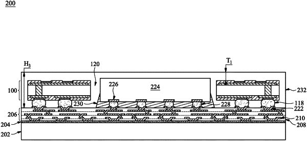
1. A package comprising:
an integrated circuit die;
a ring-shaped substrate surrounding the integrated circuit die, the ring-shaped substrate comprising a core and conductive vias extending through the core;
an encapsulant surrounding the ring-shaped substrate and the integrated circuit die, the encapsulant extending through the ring-shaped substrate, the encapsulant extending along outer sidewalls of the ring-shaped substrate; and
a first redistribution structure on the encapsulant, the first redistribution structure comprising first redistribution lines connected to the conductive vias of the ring-shaped substrate, the first redistribution structure further comprising a dielectric layer contacting the encapsulant, a top surface of the dielectric layer having a higher degree of planarity than a bottom surface of the dielectric layer.
|