| CPC H01L 23/49838 (2013.01) [H01L 21/4853 (2013.01); H01L 21/563 (2013.01); H01L 21/565 (2013.01); H01L 21/6835 (2013.01); H01L 23/3128 (2013.01); H01L 23/3135 (2013.01); H01L 23/49811 (2013.01); H01L 23/562 (2013.01); H01L 24/16 (2013.01); H01L 25/0655 (2013.01); H01L 25/50 (2013.01); H01L 2221/68331 (2013.01); H01L 2221/68372 (2013.01); H01L 2224/16227 (2013.01); H01L 2924/18161 (2013.01); H01L 2924/3511 (2013.01)] | 20 Claims |

|
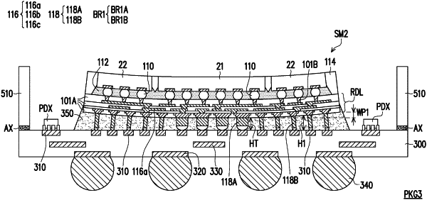
1. A structure, comprising:
a substrate;
a semiconductor package disposed on the substrate;
first bump structures and second bump structures disposed in between the substrate and the semiconductor package, and electrically connecting the substrate to the semiconductor package, wherein the second bump structures are located on at least two sides of the first bump structures, and the first bump structures and the second bump structures have different heights, and
wherein a warpage of the semiconductor package is equal to or greater than 45 μm, and the maximum width W1 of the first bump structures and the maximum width W2 of the second bump structures fulfills the following relationship: W1>W2≥0.90*W1.
|