| CPC H01L 23/49589 (2013.01) [H01L 23/49548 (2013.01); H01L 23/647 (2013.01); H01L 23/49575 (2013.01); H01L 28/10 (2013.01); H01L 28/20 (2013.01); H01L 2224/48247 (2013.01); H01L 2224/73265 (2013.01); H01L 2924/181 (2013.01)] | 20 Claims |

|
1. A method, comprising:
applying a coupling medium to an exposed lead on a surface of a leadframe substrate that includes a semiconductor die mounted on a pad of the leadframe substrate; and
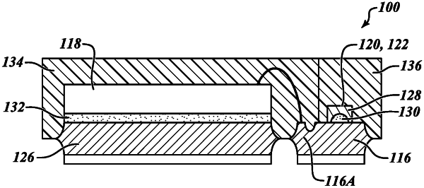
mounting a semiconductor device onto the surface of leadframe substrate by attaching an end portion of the semiconductor device to the exposed lead via the coupling medium, the end portion including a recessed member to receive at least partially the coupling medium.
|
|
15. A method, comprising:
attaching a semiconductor die onto a first surface of a carrier substrate, the carrier substrate including a plurality of metal leads surrounding the semiconductor die on the first surface of the carrier substrate;
applying a coupling medium on a first metal lead and a second metal lead of the plurality of metal leads; and
coupling a first end of a semiconductor device to the first metal lead through the coupling medium and a second end of the semiconductor device to the second lead through the coupling medium, the first end of the semiconductor device including a first recess portion facing the first metal lead, and the second end of the semiconductor device including a second recess portion facing the second metal lead.
|
|
18. A method, comprising:
locally applying an electrically conductive coupling medium on a first metal lead on a surface of a leadframe substrate that includes a semiconductor die on a pad of the leadframe substrate; and
electrically coupling an end portion of a semiconductor device to the first metal lead by at least partially receiving the electrically conductive coupling medium in a recessed portion of the end portion of the semiconductor device, wherein the recessed portion is between a first sidewall and a second sidewall of the end portion.
|