| CPC H01L 23/49517 (2013.01) [H01L 23/49 (2013.01); H01L 23/492 (2013.01); H01L 23/49513 (2013.01); H01L 23/49524 (2013.01); H01L 23/49562 (2013.01); H01L 23/53238 (2013.01); H01L 24/03 (2013.01); H01L 24/05 (2013.01); H01L 24/08 (2013.01); H01L 2224/0401 (2013.01); H01L 2224/04026 (2013.01); H01L 2224/04042 (2013.01); H01L 2224/05155 (2013.01); H01L 2224/05166 (2013.01); H01L 2224/05171 (2013.01); H01L 2224/05568 (2013.01); H01L 2224/05647 (2013.01); H01L 2224/13007 (2013.01); H01L 2224/13082 (2013.01); H01L 2224/131 (2013.01); H01L 2224/13147 (2013.01); H01L 2224/16245 (2013.01); H01L 2224/291 (2013.01); H01L 2224/32245 (2013.01); H01L 2224/73253 (2013.01); H01L 2224/73265 (2013.01); H01L 2224/81815 (2013.01); H01L 2224/92247 (2013.01); H01L 2224/94 (2013.01)] | 12 Claims |
|
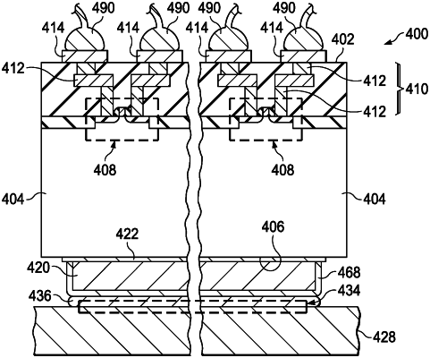
1. A microelectronic device, comprising:
a substrate having a component surface and a die attach surface located opposite from the component surface;
a wire bond attached to the component surface;
a copper containing layer on the die attach surface, wherein the copper containing layer occupies more than 50% surface area of the die attach surface; and
a die attach material on the copper containing layer, wherein the copper containing layer is attached to a portion of a lead frame by the die attach material, wherein the copper containing layer is recessed from a lateral perimeter of the die attach surface in its entirety from a bottom view of the microelectronics device.
|